| Jun 01, 2012 | Severity: Information | Eugeny Brychkov (RU) |
Do not be shocked by the title of the article - just think what 1 and 0 mean in this context. We are talking here about voltage levels of logical 0 and logical 1. They, by the TTL specifications, are defined as:
| Voltage (V) | Notes | |
|---|---|---|
| Logical level 0 (low) | 0…0,8 | Vcc=5V ± 10% |
| Logical level 1 (high) | 2…Vcc |
Note that there's a gap between 0,8 and 2 Volts, where TTL logic will be unable to identify if signal is logical 0, or logical 1. For reliable operation, such circumstances should be avoided.
As we speak about binary logical levels, binary (Boolean) logic rules should apply. The following table lists truth table for Boolean multiplication:
| A | B | A ∧ B |
|---|---|---|
| 0 | 0 | 0 |
| 0 | 1 | 0 |
| 1 | 0 | 0 |
| 1 | 1 | 1 |
You see that logical multiplication (∧) is very similar to the arithmetic one. However in digital electronics Boolean logic applies, until inputs remain digital, and device itself, or circuit built on a set of devices, produces Boolean result. Below you will see the case, which was identified and proven using GR8BIT, when binary logic gives serious flaw due to improper electrical design.
Reported by: Dominique Chuderski (FR)
When you configure GR8BIT having any active memory device in specific (sub-) slot, and put GR8BUS converter board configured within that specific slot, GR8BIT does not start. For example: putting extension ROM into the slot 3.0, and configuring converter board with jumper set into position 3.0.
Background: if two or more devices are controlled by the same signal combination and share the same bus (e.g. data bus), then they will respond to the initiator (in our case CPU) simultaneously causing electrical collision of the signals. Further in article we will discuss when such a collision is desirable, and when it may lead to the issues with operation of the system or even to the burnout of involved chips.
The rule: Outputs of different TTL gates that employ the totem-pole configuration must not be connected together since differences in their output logic will cause large currents to flow from the logic '1' output to the logic '0' output, destroying both output stages. The output of a typical TTL gate under normal operation can sink currents of up to 16 mA (ECE Lab, 2006).
There're lots of sites about TTL electronics, but only very few explicitly list this rule. It is not actually obvious that logic gates' outputs may not be connected, and the consequences of such a connection are even less obvious. We are going to closely consider the statement above, and which consequences will follow if you will not comply with the rule.
Explanation: The rule stems from the internal design of contemporary logic gates, and their output circuit in particular. Totem-pole (or push-pull, see Wikipedia) circuits comprise of two transistors, daisy-chained by their emitter-base junctions between supply voltage and ground wire. Figure 1 identifies them as Q7 and Q8. Let's assume transistor may be in two states - turned-off, when the base voltage (relative to emitter) is below cut-in voltage level and turned-on otherwise. In turned-off state current flowing through the collector-emitter junction is immaterial. In turned on-state current flowing through this junction is limited by the internal passive resistance of the transistor, and external load. As we have two transistors in the circuit shown on fig. 1, let's consider all the combinations of their states:
| # | QA | QB | Output Y | Notes |
|---|---|---|---|---|
| 0 | Off | Off | Floating (tri-state) | This state does not happen because both Q7 and Q8 are controlled by Q6 |
| 1 | Off | On | Low level (0) | Outputs logical 0 |
| 2 | On | Off | High level (1) | Outputs logical 1 |
| 3 | On | On | (see below) | Causes bridge between power line and ground |
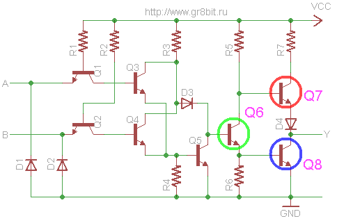
Combinations 1 and 2 represent normal TTL output of the gate. Combination 0, while it is not possible with 7432 gate shown by design, is widely used in the chips with a kind of output enable input pin, which, if activated, causes both transistors to turn-off, and release output line floating so that other device can talk to the wire without interference (those chips for instance are - bus buffers, memory chips).
Now reconsider our initial case when two TTL gates are connected together with their outputs (fig. 2). If Gates 1 and 2 are expected to output the same logical level, then either Q7/Q15 transistors are in turn-on state, or Q8/Q16. Note that if one pair is on, another will be off.
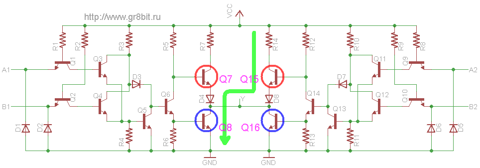
Now abstract from the particular SN7432 shown on fig.2 and imagine that, in the environment of your GR8BIT, Q7/Q8 (gate 1) represent data output stage of one of the main RAM chips, and Q15/Q16 (gate 2) represent data output stage of the data buffer located on the GR8BIT converter board. Also let's assume that main memory if located in slot 3.2 and you set converter board to the same slot 3.2. Also let's suppose that you have no cartridge installed into converter board, and main memory cell CPU is going to read contains 0.
It will happen then that gate 1 will have to output logical 0, with Q7 in turn-off state and Q8 in turn-on state, and gate 2 will have to output logical 1, with Q15 in turn-on state and Q16 in turn-off state.
There will be current Is flowing throughout Q15 and Q8. This current will be only limited by the R14 (Q15 collector's resistor), and very small internal resistance of the both transistors and diode. Of course, the read cycle time of the CPU is very small, and this collision of the electrical levels will happen for not more than 1ms, but will it cause problems with system logical operation? Let's now move to the experiment to check it.
We will assemble circuit (fig. 3) based on the bus buffer 74ALS245 (or its replica K1533AP6) using the breadboard. Bus buffer is instructed to pass signals from its channel B to channel A, thus test point TP1 is expected to be in logical level 1, and test point TP2 is expected to be in logical level 0.
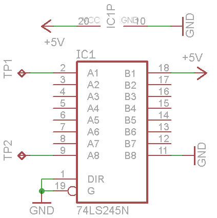
First of all, let's ensure that circuit gets the power (fig. 4) measuring potential between pins 7 (GND) and 14 (VCC) of the buffer. Then we check the voltage for the logical level 0 (low level) - on pin 9 (fig. 5), which is equal to 0.111 Volts - and is within TTL specifications.
Now we measure voltage of logical level 1 on the pin 2 (fig. 6), equal to 3.92 Volts, and is also within TTL specification. We conclude that any TTL device will reliably recognize logical 1 (data bit = 1) on the buffer's pin 2, and logical level 0 (data bit = 0) on the buffer's pin 9.
In our experiment we are going to check what will happen if TP1 and TP2 are shorted. Before shorting them, let's check voltage between them (fig. 7). We find out that it is exactly the difference between voltages of logical level 1and logical level 0 - 3.79 Volts.
 Figure 4. Measuring circuit's input power |
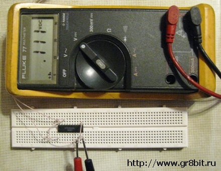 Figure 5. Measuring voltage of logical level 0 | |
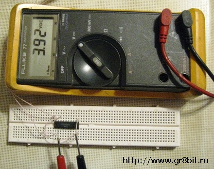 Figure 6. Measuring voltage of logical level 1 |
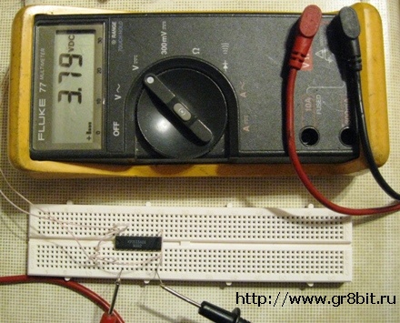 Figure 7. Measuring voltage between TP1 and TP2 | |
Important: the following actions are performed in order to show the outcomes of specific situation within the circuit, they cannot be treated as guidance for action. There're specific hazards related to the reproduction of test.
Now we are going to short-circuit TP1 and TP2, and see the value of the current flowing between them. We use ammeter built into the multimeter (fig. 8). We found out that current flowing between these test pads is 97 mA. Looking to the datasheet we see that, for SN74ALS245, maximal low-level output current IOL is 24 mA, and we have quadruple excess of maximal current for the gate!
Having TP1 and TP2 steadily shorted in this test, chip has heated considerably to the 70°C within seconds, and its electrical and logical characteristics started to slide (from the datasheet we see that recommended maximal free-air temperature is 70°C - and proper chip functioning above this level is not guaranteed).
But what is about voltage, and logical levels on the wire which shorts points TP1 and TP2? Figure 9 shows we have measured it to be 0.892 Volts, which is out of the TTL specification. This is not logical zero, while is very close to it. CPU will have difficulties identifying what the resulting logical level is, and the truth table of logical multiplication does not apply. As chip heats voltage starts to slowly slide in the direction of 0.8 Volts, however it is very probable that this chip will fry before it will reach defined logical 0. In addition, during the read cycle, CPU will not wait until logical level on some its data line will become valid. It will just somehow decide, and will probably be wrong - making whole system misbehaving.
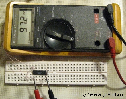 Figure 8. Measuring the current between TP1 and TP2 |
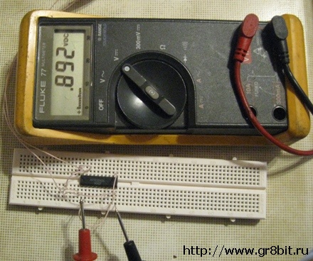 Figure 9. Measuring voltage on shorted TP1 and TP2 |
Do not force two or more devices talking onto the bus line simultaneously setting them into the same real or virtual address space. This causes electrical conflict, and invalidates any data being read by CPU. Even if it looks like you do not have any cartridge in the converter board, you actually have bus buffer there which outputs high level onto the data bus when being read.
The only exception is circuit with devices having open collector outputs, which are specially designed to operate in shared output designs. You can see these open collector implementations in CPUINT and CPUWAIT signal generation circuits.
End of KB0007 "When and why 1 multiplied by 0 is not equal to 0".
| © 2011-2024 Eugeny Brychkov | http://www.gr8bit.ru | Status: Released |
 |
|||||

|

|
GR8BIT™, GR8BOOK™, GR8BUS™, GR8BOX™, GR8STORM™ and GR8NET™ are trademarks
copyright © 2010-2024 Eugeny Brychkov.
Please refer to: copyright statement,
privacy policy.