| Dec 03, 2012 (initial release of Nov 26, 2012) | Severity: Information | Eugeny Brychkov (RU) |
With the emergence of the GR8BUS master board we introduce contemporary advanced technology of the virtual circuit design experience, programming, and even more fun than ever. Programming the FPGA device is very similar to the designing and creating circuit diagrams - like we did for GR8BIT - at the very simple level, and dynamically configuring the created circuit diagrams into the chip.
If you were able, by your own or with the help of community, to build and start your GR8BIT, you will stretch your experience beyond that by touching FPGA experience, starting from the very basics, and probably ending with your own projects or contributions to the wider projects.

Warning: do not connect GR8BUS master board and PC using ByteBlaster-II device when power is applied to your GR8BIT platform. Even more, it is not just about power being turned on, but about grounding. In ungrounded state (or improper grounded state) potential between GR8BIT and PC can reach up the value of the AC power you have in the outlet. To be safe - disconnect GR8BIT's power cord from the power mains and other power and ground sources before connecting the systems.
Exactly this way - connecting GR8BUS master board and PC "on-the-fly" - we fried (damaged) Cyclone-III chip's JTAG interface of the prototype of GR8BUS master board. For grounding considerations please refer to GR8BOOK part III, section 1.4 Protective grounding.
In order to simplify the design of the GR8BUS master board, we designed it to have JTAG configuration and ByteBlaster-II interfaces. You may use your own USB-Blaster device, connecting to these two ports if you wish.
The differences between these two interfaces are:
The best practice is that during development of the configuration, when you modify code, re-compile and need to try what you have done in hardware, you use JTAG mode. When you finished some stage of your development, and need configuration to be present in the FPGA device on power cycle, you use Active Serial mode flashing configuration to the configuration device.
If you will Google for "byteblaster circuit diagram" you will see many diagrams, which are claimed to be working. However if you will consult official Altera's ByteBlaster-II guide, you will see that most of those circuit diagrams do not represent full functionality of ByteBlaster-II device (see user guide, p.2-2). These limited implementation of ByteBlaster-type interface, while should be working configuration, actually provides limited functionality - you will not be able to use them to use it in Active Serial programming mode, which requires nCE and nCS signals to be present in the ByteBlaster bus (see user guide, p.2-3 and p.2.4, table titled ByteBlaster II Female Plug Signal Names and Programming Modes).
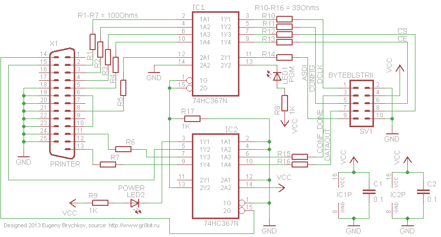
Our ByteBlaster-II interface will provide full functionality, implementing all the lines shown on the block diagram in the user guide.
Circuit diagram is shown on the fig.1. It uses a number of identical components: two 74HC367N chips, 7 resistors of 100Ohms, 7 resistors of 33Ohms, three resistors of 1KOhms, two LEDs, two connectors (DB-25M and BH-10R), two decoupling capacitors of 0.1µF. It also uses a box of the DB25-to-DB25 converter, and a small piece of breadboard.
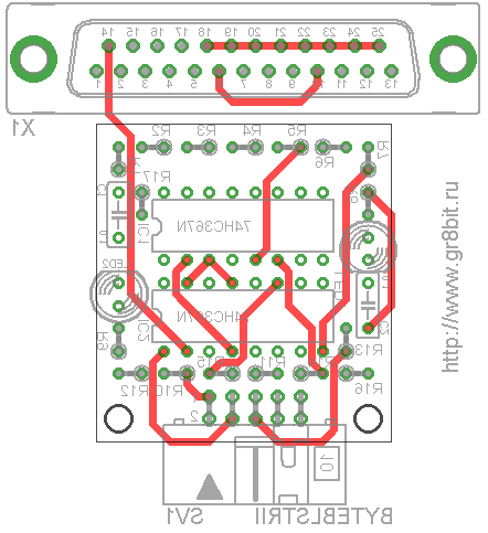
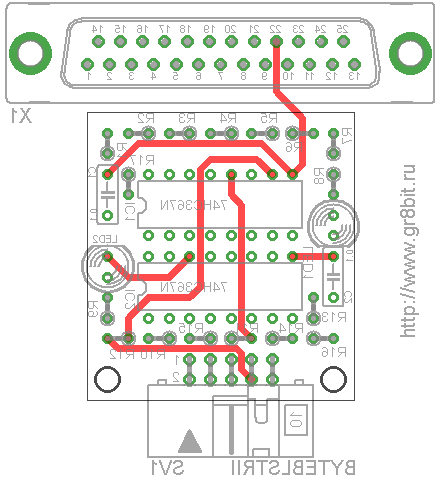
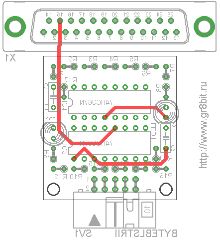
We provide the manufacturing process for your reference (fig.2), you may decide to take different size of the breadboard, or locate components different on it in order to have more convenient soldering. Sample pictures are shown on the fig.3.
IC1 provides buffered signal output in the direction from PC's parallel port to the GR8BUS master configurable device (5 signals). These output signals are enabled by the inverted signal from parallel port's pin 14 (it goes to output enable of the second element of IC2 and its output 13 provides inverted signal to the IC1 - R17 is a pull-down resistor to ensure low level of the IC1's inputs 1 and 15 when IC2's input 15 is high - second element of IC2 is disabled). First element of IC2 is buffered signal input from GR8BUS master configurable device to PC's parallel port (2 signals). Resistors R1-R7 and R10-R16 are used to limit current flow and as termination elements for relatively long-distance wires.
 (a) Wiring, stage 1 |
 (b) Adding wiring, stage 2 | |
 (c) Adding wiring, stage 3 |
 (d) Adding wiring, stage 4 | |
| Figure 2. Wiring process (view from the soldering side). Adjacent pins can be shorted with a solder instead of air-wire. Board size is 12*14 pads. | ||
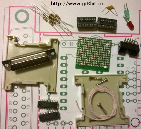 A set of components |
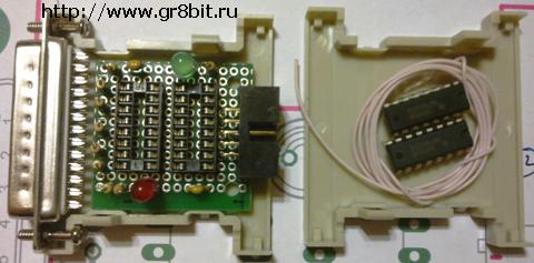 Components soldered in | |
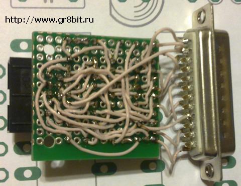 Almost all air-wires are soldered | ||
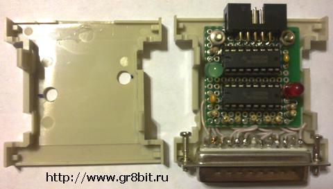 Device assembled |
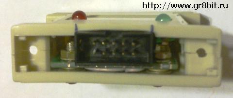 View from the ByteBlater-II interface side | |
| Figure 3. Our ByteBlaster-II device Device pictures shown are not of a final design. Final design is presented on fig.1 (circuit diagram) and fig.2 (air-wiring) of this KB0011. Pictures are for your reference only. | ||
End of KB0011 "Building ByteBlaster-II device".
Re-release of Dec 03 2012: added warning about interconnecting GR8BIT and PC and grounding.
| © 2011-2024 Eugeny Brychkov | http://www.gr8bit.ru | Status: Released |
 |
|||||

|

|
GR8BIT™, GR8BOOK™, GR8BUS™, GR8BOX™, GR8STORM™ and GR8NET™ are trademarks
copyright © 2010-2024 Eugeny Brychkov.
Please refer to: copyright statement,
privacy policy.