| Mar 03, 2014 | Severity: Information | Daisuke Shiraishi (白石大介, JP), Eugeny Brychkov (RU) |
Our SDRAM controller provides independent channels to connect two devices. Both connected devices are able to access whole memory space of the SDRAM, and it is up to designer to implement logical separation of the memory space, or design pseudo-dual-port access to the memory. Controller is designed to operate time-sharing algorithm for three operation: two time slots for two channels, and one internal time slot for memory refresh. Maximal time required for memory read/write completion is 280 nanoseconds. Controller provides busy signals to connected devices. Controller operates at 85.92MHz clock speed.
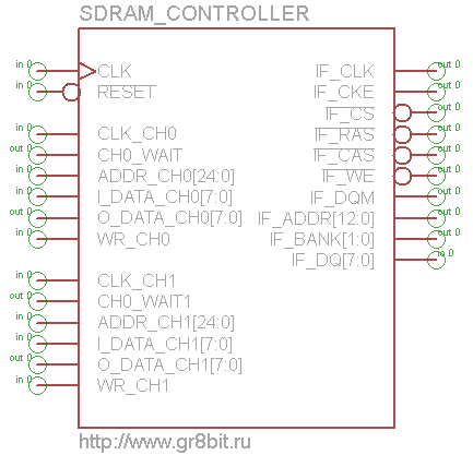
SDRAM controller can be described as a logical component depicted on the fig. 1. Control is provided by supplying main clock to the CLOCK pin, and RESET signal to the respective pin. All controller's internals function on the falling or rising edge of the clock. If clock stops, SDRAM will lose its contents due to no refresh.
Channels 0 and 1 have independent input and output pins. External device should ensure that CHx_WAIT pin is low before raising CLK_CHx. Controller synchronizes CLK_CHx signal with CLK internally, thus length of CLK_CHx being active should be at least one cycle of the CLK. All channel input data should be stable prior raising CLK_CHx signal. After request for operation is registered, controller raises CHx_WAIT signal, which remains active until respective read or write cycle is complete. In case of read operation, when CHx_WAIT signal goes inactive, O_DATA_CHx lines contain valid data read from the memory. Signal SW_CHx is an input signal signalling to controller if operation requested will be read (low) or write (high).
IF_ pins are interface to the SDRAM chip. Controller was designed for the Micron MT48LC32M8A2-75, its datasheet can be found at the manufacturer's website. Please note that there're various revisions of datasheet exists, we used datasheet labelled "256Mb_sdr.pdf - Rev. V 01/14 EN". You should always use latest version of datasheet as we found several, from our point of view, significant difference with earlier versions (in particular - in power up sequence and timing).
Maximal allowed CLK clock frequency in this implementation is 90MHz (thus 85.92MHz is very close to the limit). Going above 90MHz will violate -75 type chip timing, and controller will need to be redesigned.
During reset no memory refresh if performed, and resetting the controller for extended period of time more than 60µs will cause SDRAM data loss.
There're specific predefined actions controller should perform in order to initialize SDRAM into the state it is expected to function. Trigger of the initialization (or re-initialization) sequence is RESET signal going active (low). Sequence is very well explained in the SDRAM datasheet.
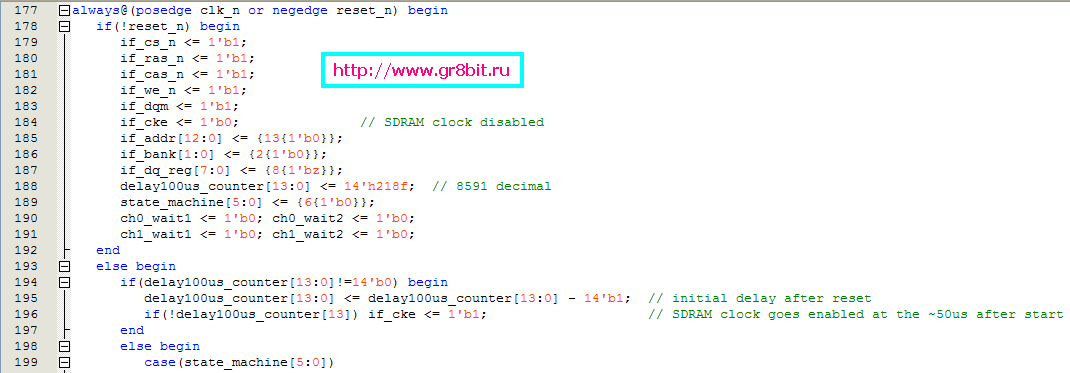
Lines 179-191 initialize pins connected to SDRAM to the defined level (except data DQ pins). After RESET is released, execution starts with 8591 wait cycles (100µs), with CKE disabling SDRAM clock at the beginning, and then enabling it in the middle of the wait cycle execution (line 196). When counter delay100us_counter reaches zero, command execution starts.
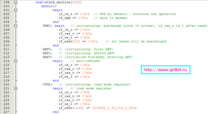
First command executed is PRECHARGE for all banks (needs A10 to be set to 1). Second and third are both same AUTO-REFRESH (ARF) commands. The last one is LMR (load mode register, CFGL) command, which sets up SDRAM to have single byte read and write bursts, and sets CAS latency time to 2. Mode register is extremely important to perform properly, otherwise SDRAM will not function properly. Note than BA[1:0] signals are driven low during LMR command (implicitly, reset during reset event in line 186).
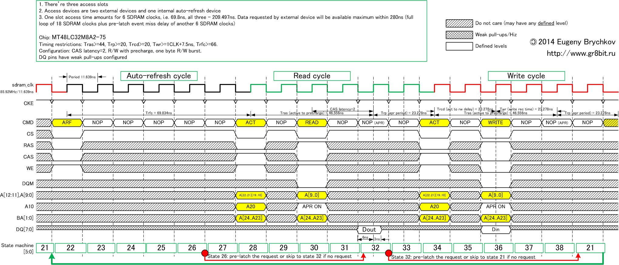
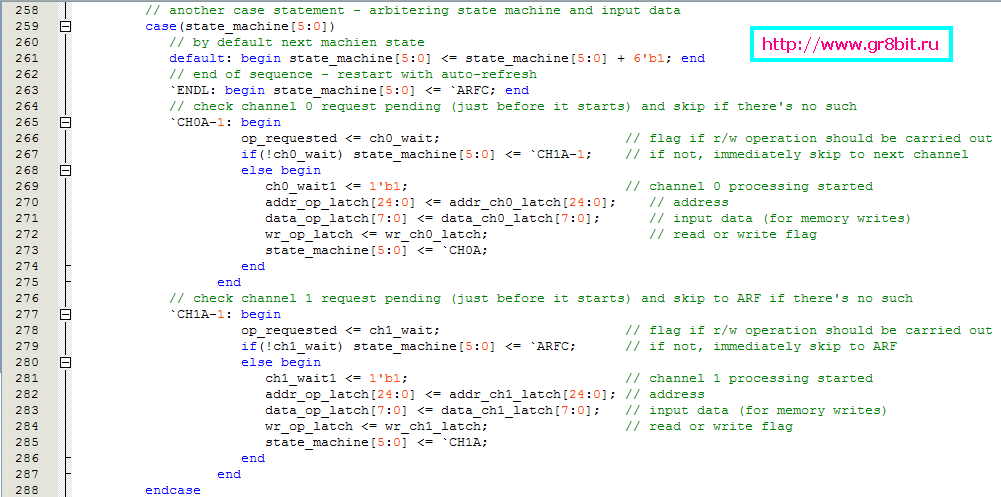
Figure 4 shows main access state machine timing with the SDRAM. Every loop AUTO-REFRESH (ARF) command is executed (line 213, fig. 3). It lengths for 6 cycles, amounting for about 70 ns (minimal for -75 chip type is 66 ns). Just before the channel 0 activity (CH0A-1, state 26, falling edge of the clock, marked with red circle on fig. 4) controller checks if there's I/O request pending (line 266). If there is, it raises next busy flag (wait1), loads input data to the registers (performs pre-load) which will then be put onto SDRAM pins, and goes to the state 27 (CH0A). However if there's no request pending for channel 0, it immediately skips to the CH1A-1 state to serve channel 1 the same exactly way (line 267 on fig. 5, and red arrow on fig. 4). And if there's no request pending for channel 0, execution skips to state 21 - auto-refresh.
During execution of write command, data is put onto SDRAM DQ pins at the write command cycle, and then removed. In order to keep SDRAM data lines stable it is important to active pull-ups for them. During execution of read command, data is read from the SDRAM DQ pins at the rising edge of the SDRAM clock, and put into the output register to be read by the device attached to the controller.
If access request was detected and wait1 flag was raised, there will be another flag wait2 raised at the end of the operation, which will them be sampled in the access control block, and if raised, will reset master busy flag CHx_WAIT.
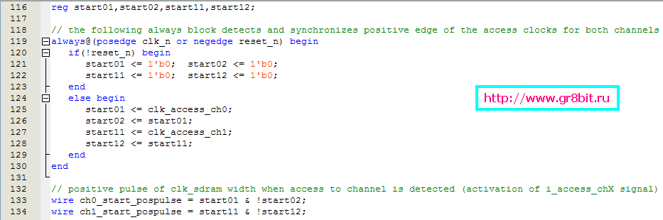
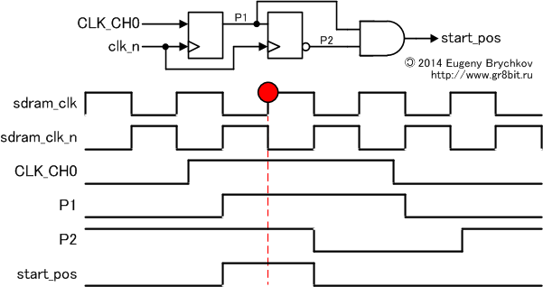
Figure 6 shows configuration of two synchronization circuits within single always block - for both channel 0 and 1. It is built on two flip-flops, driven by the negative edge of SDRAM clock (positive edge of negated SDRAM clock clk_n), giving positive-edge impulse at its output of the length equal to the cycle of the SDRAM clock (fig. 7). SDRAM controller, on the rising edge of SDRAM clock, detects level of the start pulse (designated with the red circle), latches request details from the respective channel's pins, and schedules its processing raising CHx_WAIT signal.
End of KB0016 "Dual port SDRAM controller".
| © 2011-2024 Eugeny Brychkov | http://www.gr8bit.ru | Status: Released |
 |
|||||

|

|
GR8BIT™, GR8BOOK™, GR8BUS™, GR8BOX™, GR8STORM™ and GR8NET™ are trademarks
copyright © 2010-2024 Eugeny Brychkov.
Please refer to: copyright statement,
privacy policy.